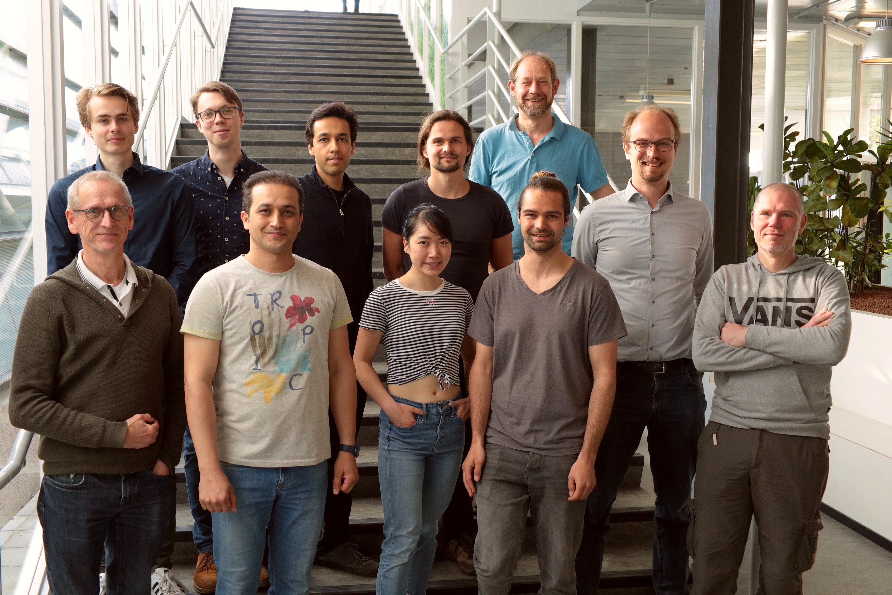
Sense Jan van der Molen Lab - Physics of Quantum Materials
In our lab, we investigate the physics and material properties of low-dimensional systems.
One-dimensional quantum systems (molecules)
Historically, the group started out investigating charge transport (conductance) through molecules. You can consider molecules as quasi one-dimensional quantum systems, with properties that are tunable by chemical synthesis. We have always had a specific interest in functional molecules, e.g. photochromic switches and spin-crossover compounds. Part of this work has been done in collaboration with Prof. Ben Feringa (Nobelprize winner in Chemistry) in Groningen
Recently, our focus of molecular research has shifted somewhat from single-molecular junctions, towards 2D-systems based on thin (monolayer) molecular films (PhD student Arash Tebyani). For chiral molecular layers, we are studying spin selectivity (chirality-induced spin selectivity - or CISS - effect, PhD student Peter Neu), in a nation-wide collaboration that includes Jan van Ruitenbeek (Leiden) and Herre van der Zant (TU Delft).
Two-dimensional quantum systems (van der Waals materials)
A significant research effort in our group concerns the electronic properties of and charge transport through quasi two-dimensional systems. The most famous of these is undoubtedly graphene--a carbon layer of exactly one atom thick. But there are many more, such as hexagonal BN and MoS2. Remarkably, such layers can be stacked to create novel materials--called Van der Waals materials--with properties that we may be able to tune in the future. This would open the door to so-called ‘designer materials’.
To reach that point one day, we are accurately investigating the electronic interaction between different layers within Van der Waals materials (PhD students Tobias de Jong and Xing Chen (also in Michiel de Dood’s group)). We have a unique way to do this, thanks to our low-energy electron microscope (LEEM), which is a spectroscope at the same time! Moreover, we have adapted the system to our needs. Recently, this has enabled us to locally pinpoint magic-angle areas in twisted bilayer graphene. Moreover, in a collaboration with Milan Allan, Felix Baumberger - Geneva and Dima Efetov - ICFO we have presented evidence for flat electronic bands in magic-angle areas, as reported in Nature Physics. We are currently intensifying our research in this direction.
LEEM
Our work horse is a low-energy electron microscope (LEEM) called ESCHER. Due to its aberration correction, it has a record lateral resolution of 1.4 nm. Still, our research program aims far beyond pure microscopy. One of our goals has been to make LEEM a key measurement system in condensed matter physics research as a whole and to apply it specifically for research on Van der Waals materials, thin oxides and molecular. For that reason, we have recently introduced various new techniques:
- LEEM-based potentiometry (LEEP), allowing us to map potential differences in a 2D material under a voltage bias.
- Angle-resolved reflected-electron spectroscopy (ARRES) which allows us to map the dispersion of unoccupied bands above the vacuum level with a very high cross section.
- A novel form of transmission electron microscopy operating at very low energies, i.e. 0-100 eV (hence named eV-TEM)
As a result, 'LEEM' has actually become an umbrella term for a measurement system that incorporates a plethora of unique techniques that can be used in real-time (these also include (micro)LEED, dark-field imaging and (micro)ARPES).
ONEM
As of January 1, 2021, we are developing a new form of microscopy, in a European FET collaboration with Thomas Juffmann (U Vienna) and Mariana Amaro (HIPC, Prague). The new type of microscopy combines the best of optical microscopy (no damage to organic, biological structures) with the best of electron microscopy (a superb resolution). We have coined it ONEM (optical near-field electron microscopy). Currently, we are starting our efforts, which includes collaborations with and contributions from SPECS GmbH (Berlin) and RMD Inc. (USA). The Leiden team includes a new PhD student (Guido Stam), Prof. Ruud Tromp (IBM and Leiden), a technician, and a postdoc.

News
-
 Hooray! This extremely sensitive microscope survived its relocation
 -
 Physicist Sense Jan van der Molen plays ‘Dutch shuffleboard’ with electrons
 -
 New ONEM Microscope to combine best of two worlds
 -
 First NWO Communication Award for Leiden Wall Formula project
 -
 8th wall formula about the Van der Waals-equation for gases
 -
 Superconductivity with a twist explained
 -
 LION in lockdown
 -
 Stacked graphene layers act as a mirror for electron beams
 -
 Leiden involved in three out of five Physics Vrije Programma grants
Key publications
-
Geelen D., Jobst J., Krasovskii E.E., Molen S.J. van der & Tromp R.M. (2019), Nonuniversal transverse electron mean free path through few-layer graphene, Physical Review Letters 123(8): 086802.
-
Atesci H., Kaliginedi V., Celis Gil J.A., Ozawa H., Thijssen J.M., Broekman P., Haga M. & Molen S.J. van der (2018), Humidity-controlled rectification switching in ruthenium-complex molecular junctions, Nature Nanotechnology 13: 117-121.
-
Thete A., Geelen D., Molen S.J. van der & Tromp R.M. (2017), Charge catastrophe and dielectric breakdown during exposure of organic thin films to low-energy electron radiation, Physical Review Letters 119(26): 266803.
-
Jobst J., Torren A.J.H. van der, Krasovskii E.E., Balgley J., Dean C.R., Tromp R.M. & Molen S.J. van der (2016), Quantifying electronic band interactions in van der Waals materials using angle-resolved reflected-electron spectroscopy, NATURE COMMUNICATIONS 7: 13621.
-
Jobst J., Kautz J., Geelen D., Tromp R.M. & Molen S.J. van der (2015), Nanoscale measurements of unoccupied band dispersion in few-layer graphene, NATURE COMMUNICATIONS 6: 8926.
-
Molen S.J. van der & Liljeroth P. (2010), Charge transport through molecular switches, Journal of Physics : Condensed Matter 22: 133001.


